← Troubleshooting Commercial Light Systems With A Lighting Contactor Wiring Diagram With Photocell And Snog Wiring Schematics - Square d lighting contactor class 8903 wiring diagram Improve Your Presentations With A Diagramme Flux Powerpoint Created Using A Reliable Wiring Diagram Online Platform Today - Chronologie 3 4 5 6 7 options infographie pour les présentations ... →
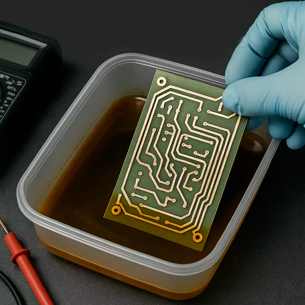
If you are searching about What is PCB Etching and Its Process Flow? - TechSparks you've came to the right page. We have 35 Pics about What is PCB Etching and Its Process Flow? - TechSparks like PCB-Investigator Ultimate | PCB Design Tools, DIY home PCB exposure and etching process | Just Add Electrons and also DIY home PCB exposure and etching process | Just Add Electrons. Here you go:
What Is PCB Etching And Its Process Flow? - TechSparks
 www.tech-sparks.com
What is PCB Etching and Its Process Flow? - TechSparks
CAE Data For PCB Engineering | Phoenix Contact
 www.phoenixcontact.com
CAE data for PCB engineering | Phoenix Contact
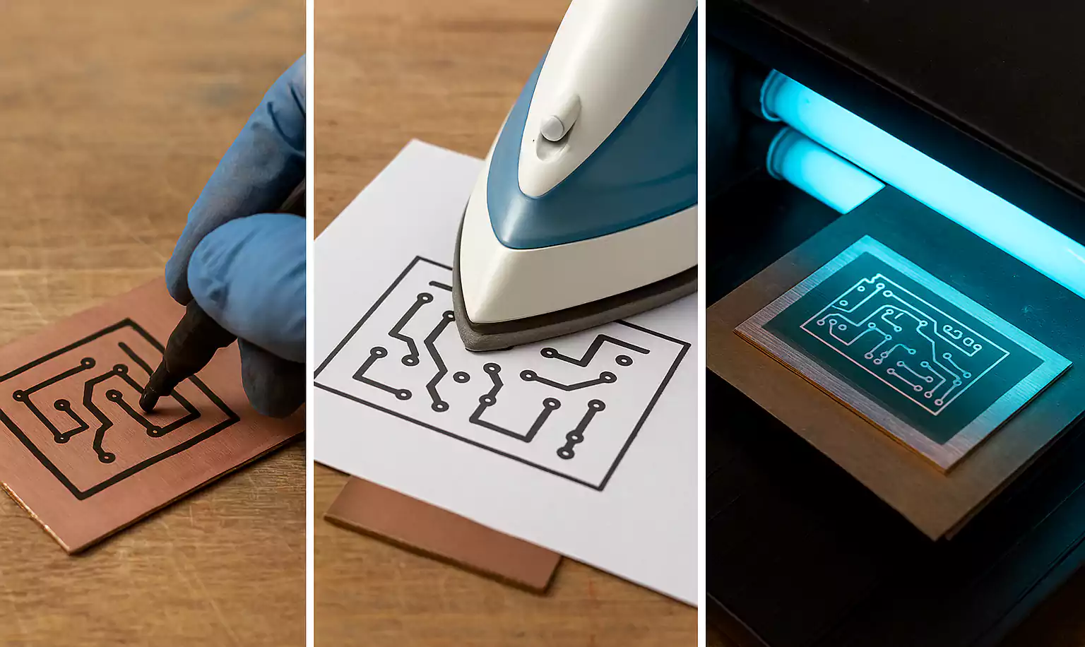
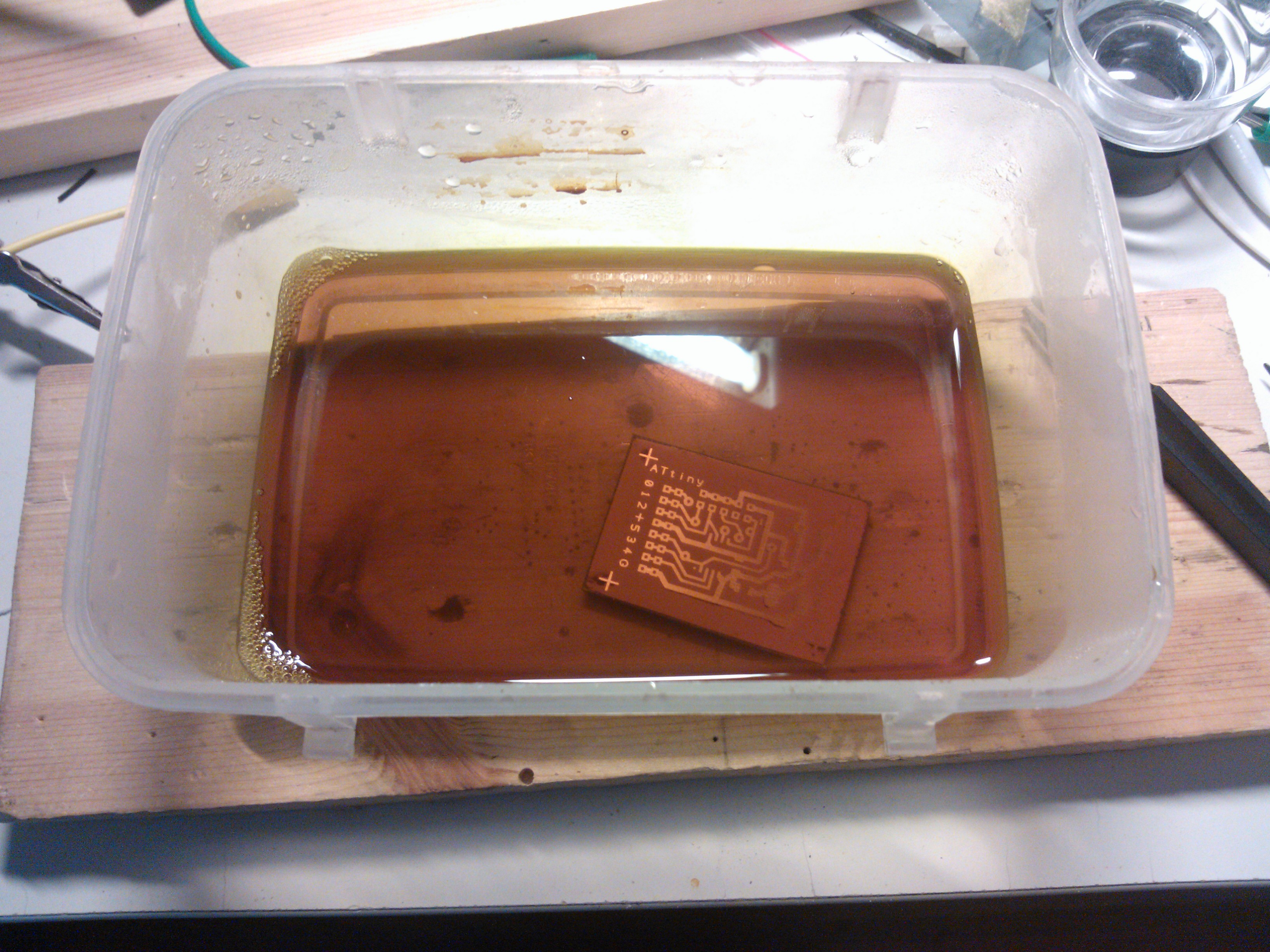
DIY Home PCB Exposure And Etching Process | Just Add Electrons
 justaddelectrons.com
DIY home PCB exposure and etching process | Just Add Electrons
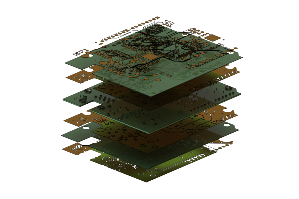
PCB Reverse Engineering: Comprehensive Guide For Beginners
 www.fscircuits.com
PCB Reverse Engineering: Comprehensive Guide for Beginners
Top 7 PCB Layout Design Software For Beginners - IBE Electronics
 www.pcbaaa.com
Top 7 PCB layout design software for beginners - IBE Electronics
10 Essential PCB Design Software Tutorials For Beginners
 tryvary.com
10 Essential PCB Design Software Tutorials for Beginners
PCB Etching - A Complete Guide - PCBA Manufacturers
 www.pcba-manufacturers.com
PCB etching - a complete guide - PCBA Manufacturers
PCB Health Effects: PCB Exposure Symptoms & Risks
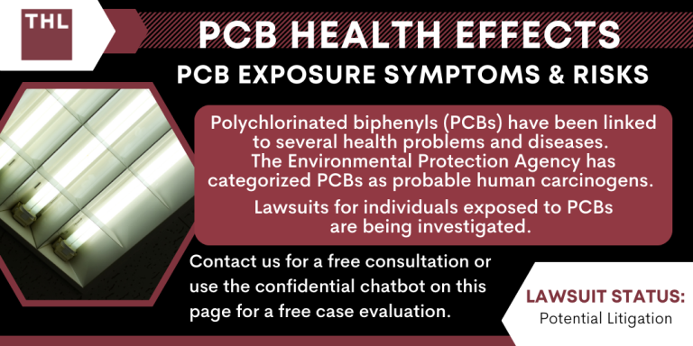 www.torhoermanlaw.com
PCB Health Effects: PCB Exposure Symptoms & Risks
PCB Silkscreen: The Ultimate Guide For Beginners
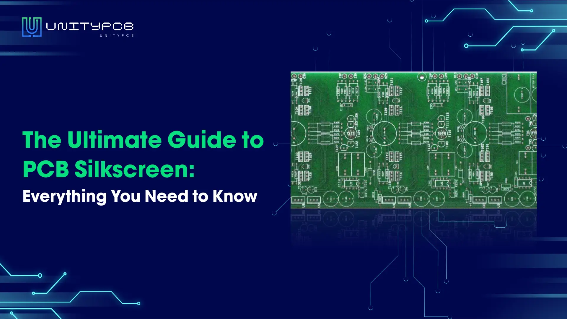 unitypcb.com
PCB Silkscreen: The Ultimate Guide for Beginners
LED Exposure Machine For PCB Circuit And Solder Mask - Photo Chemical
 www.etching-machine.com
LED exposure machine for PCB Circuit and solder mask - photo chemical ...
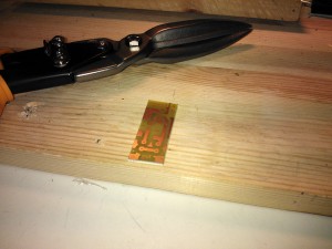
DIY Home PCB Exposure And Etching Process | Just Add Electrons
 justaddelectrons.com
DIY home PCB exposure and etching process | Just Add Electrons
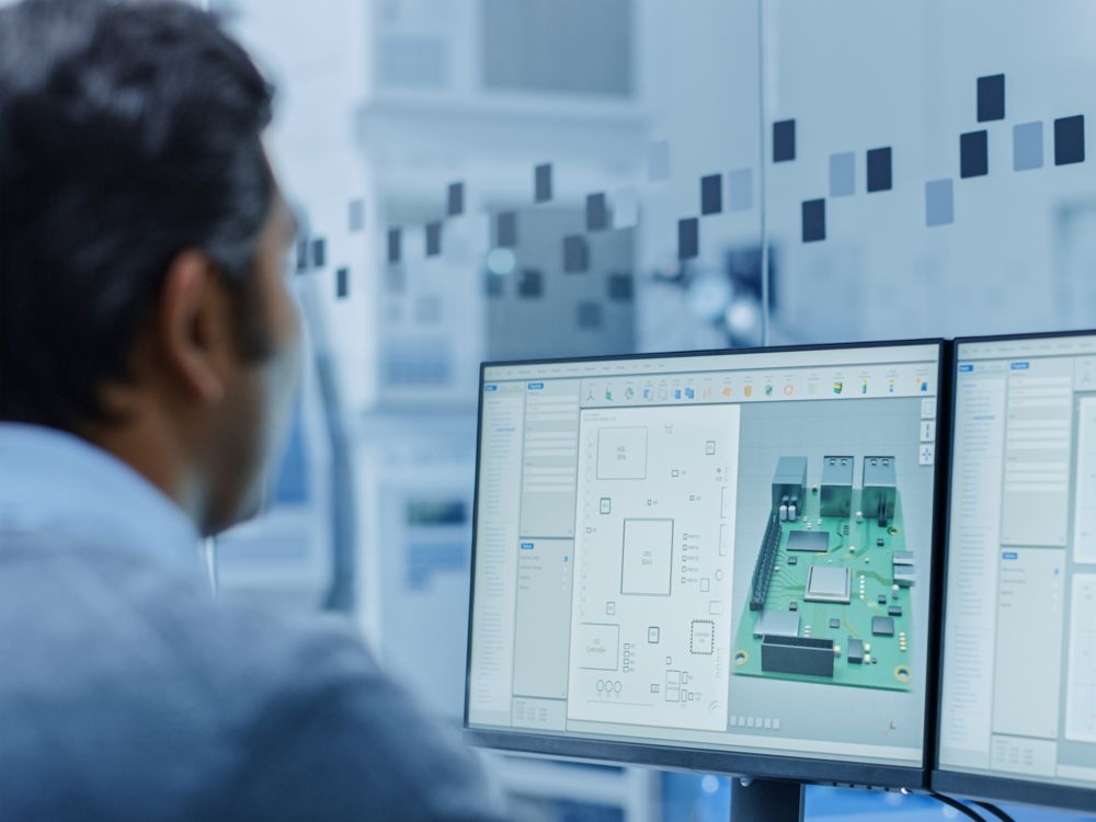
PCB-Investigator Ultimate | PCB-Design Tools
 www.pcb-investigator.com
PCB-Investigator Ultimate | PCB-Design Tools
DIY Home PCB Exposure And Etching Process | Just Add Electrons
 justaddelectrons.com
DIY home PCB exposure and etching process | Just Add Electrons
Fun Tips About What Chemical Is Used For Pcb Etching Blog | Adimmix
 adimmix.com
Fun Tips About What Chemical Is Used For Pcb Etching Blog | Adimmix
Ceramic PCB|Flex PCB|FR4 PCB|Metal Core PCB|PCB Manufacturing-Best
 www.bestpwb.com
Ceramic PCB|Flex PCB|FR4 PCB|Metal Core PCB|PCB Manufacturing-Best ...
PCB Etching Process Explained: DIY Methods Vs. Industrial Techniques
 www.fastturnpcbs.com
PCB Etching Process Explained: DIY Methods Vs. Industrial Techniques
How Do You Test For PCB Exposure? [2026 Guide]
![How Do You Test For PCB Exposure? [2026 Guide]](https://trulawsuitinfo.com/wp-content/uploads/2024/01/Testing-for-PCB-Exposure-and-Contamination.png) trulawsuitinfo.com
trulawsuitinfo.com
How Do You Test For PCB Exposure? [2026 Guide]
10 Best Free PCB Design Software For Beginners - Mainpcba One-stop PCB
 www.mainpcba.com
10 Best Free PCB Design Software for Beginners - Mainpcba One-stop PCB ...
DIY Home PCB Exposure And Etching Process | Just Add Electrons
 justaddelectrons.com
DIY home PCB exposure and etching process | Just Add Electrons
How To Avoid PCB Exposure [2025 Update]
![How To Avoid PCB Exposure [2025 Update]](https://trulawsuitinfo.com/wp-content/uploads/2024/01/Effective-PCB-Exposure-Prevention.png) trulawsuitinfo.com
trulawsuitinfo.com
How To Avoid PCB Exposure [2025 Update]
Laser Exposure Machine Makes PCB More Efficient - RayMing PCB
 www.raypcb.com
Laser Exposure Machine Makes PCB More Efficient - RayMing PCB
The Importance Of PCB Inspection - JW Corp
 thejwcorp.com
The Importance of PCB Inspection - JW Corp
PCB Exposure Pathways: Understanding Environmental Fate | TruLawsuit Info
 trulawsuitinfo.com
PCB Exposure Pathways: Understanding Environmental Fate | TruLawsuit Info
DIY Home PCB Exposure And Etching Process | Just Add Electrons
 justaddelectrons.com
DIY home PCB exposure and etching process | Just Add Electrons
PCB Solder Mask Exposure System - Photo Chemical Etching Machine
 www.etching-machine.com
PCB solder mask exposure system - photo chemical etching machine
Ultimate PCB Design Guide: A Game-Changer!
 www.szyunze.com
Ultimate PCB Design Guide: A Game-Changer!
Laser Etching PCB: A Comprehensive Guide For Beginners - MorePCB
 morepcb.com
Laser Etching PCB: A Comprehensive Guide for Beginners - MorePCB
Qualifying For A PCB Exposure Lawsuit: Key Factors [2026 Guide]
![Qualifying For A PCB Exposure Lawsuit: Key Factors [2026 Guide]](https://trulawsuitinfo.com/wp-content/uploads/2024/02/Criteria-for-Qualifying-for-a-PCB-Exposure-Lawsuit.png) trulawsuitinfo.com
trulawsuitinfo.com
Qualifying For A PCB Exposure Lawsuit: Key Factors [2026 Guide]
How To Avoid PCB Exposure [2025 Update]
![How To Avoid PCB Exposure [2025 Update]](https://trulawsuitinfo.com/wp-content/uploads/2024/01/How-To-Avoid-PCB-Exposure-1.png) trulawsuitinfo.com
trulawsuitinfo.com
How To Avoid PCB Exposure [2025 Update]
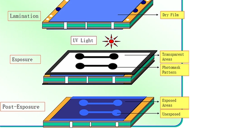
What Is Exposure In PCB Production - Fastlink PCB
 www.fastlink-electronics.com
What Is Exposure in PCB Production - Fastlink PCB
PCB Etching - A Complete Guide - PCBA Manufacturers
 www.pcba-manufacturers.com
PCB etching - a complete guide - PCBA Manufacturers
What Is Exposure In PCB Production - Fastlink PCB
 www.fastlink-electronics.com
What Is Exposure in PCB Production - Fastlink PCB
PCB Etching Process Explained: DIY Methods Vs. Industrial Techniques
 www.fastturnpcbs.com
PCB Etching Process Explained: DIY Methods Vs. Industrial Techniques
DIY Home PCB Exposure And Etching Process | Just Add Electrons
 justaddelectrons.com
DIY home PCB exposure and etching process | Just Add Electrons
PCB-Investigator Ultimate | PCB Design Tools
 www.pcb-investigator.com
PCB-Investigator Ultimate | PCB Design Tools
Ceramic pcb|flex pcb|fr4 pcb|metal core pcb|pcb manufacturing-best .... pcb-investigator ultimate. Diy home pcb exposure and etching process